 中文
中文usage of silicon wafer slag
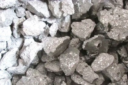
The industrial chain of the photovoltaic industry includes the process from polycrystalline silicon, monocrystalline silicon to solar photovoltaic panels. From monocrystalline silicon ingots to photovoltaic panels, a series of processing processes are required. These processing processes will produce various Silicon wafer slags, the most important of which is Silicon wafer. The slag production process is the process of pulling the silicon rod and slicing the silicon ingot, etc. The Silicon wafer slag produced by these two processes is generally called the crystal-pulling Silicon wafer slag and the slicing Silicon wafer slag. It is cut into silicon wafers, the silicon powder produced in the process enters the water, and the sewage containing silicon powder is precipitated and filtered to form a silicon mud. The water content of this silicon mud is usually 45-60%. The silicon content of the two silicon wafer slags is different. , the silicon content of crystal pulling is low, the silicon content (all silicon) in the dry base composition is 60-80%, the elemental silicon content is 35-65%, and the silicon wafer slag silicon content (all silicon) is 85-97%, The elemental silicon content is 70-95%.
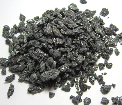
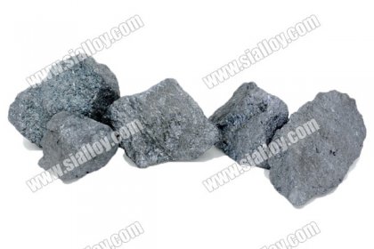
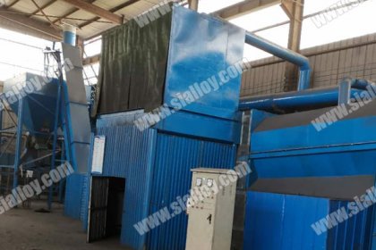
Silicon wafer slag in photovoltaic industry has the largest output of sliced Silicon wafer slag, accounting for about 85-90% of the total amount of Silicon wafer slag, and the annual output of 1GW silicon wafer (182 wafers) is 55-60% water content. Silicon wafer slag1800 tons or so. In 2021, the domestic silicon wafer production will be about 227GW. If calculated on an average of 182 wafers, the annual Silicon wafer slag production will be about 400,000 tons. At present, domestic enterprises that use sliced Silicon wafer slag mainly use the method of intermediate frequency furnace smelting. After the Silicon wafer slag is dried, it is smelted in the intermediate frequency furnace to produce metal silicon products. Including Silicon 3303, Silicon 441, Silicon 553 and other models. Silicon is a semiconductor and has almost no magnetism at room temperature. The melting point of silicon is very high, reaching 1436 ° C. After the metal silicon forms a liquid, it has the magnetic properties of liquid metal, so induction can be used. The heating method is used to melt and heat up, but the silicon powder is from room temperature to the melting temperature of metal silicon at 1436 ° C. Since there is no magnetism, induction heating cannot be achieved in this temperature range. Therefore, it is necessary to spread a small amount of coke or waste electrode blocks at the bottom of the intermediate frequency furnace in advance. A single graphite electrode is inserted into the intermediate frequency furnace.
After electrification, a short circuit is formed between the electrode and the coke to achieve arcing. After the arcing is successful, a small amount of silicon powder is added to the electrode arc in several times. Melt to form silicon water. After a certain depth of silicon water is formed in the intermediate frequency furnace, generally 15-20% of the depth, the electrode is taken out. Since there is silicon water that can conduct magnetic fields in the furnace, the induction heating of the intermediate frequency furnace begins to play a role. The silica fume gradually melts. In the production process, like other silicon metal, a large number of silicon slag as a by-product, will be produced.
Main Products
Hot Products
Blog
Contact Us
Business Add: 15F, 1511, Yi Wu Trade Building, Wenfeng Avenue, Anyang, Henan, China.
Factory Add: Industrial Park of Dong zhang wu, Qugou Town, Anyang City, Henan Province, China.
Tel: (86) 372 5039979Fax: (86) 372 5039931
Postcode: 455000
E-mail: [email protected]
Factory Add: Industrial Park of Dong zhang wu, Qugou Town, Anyang City, Henan Province, China.
© Anyang Huatuo Metallurgy Co., Ltd.